2026-02-12

This guideline helps you to create a PCB that is ready for production test.
Designing a PCB with production testing in mind is essential for achieving high yield, reliable measurements, and cost-efficient manufacturing. Whether you are defining how to test a PCB board or working together with circuit board testers and fixture manufacturers, early design decisions have a major impact on the quality and stability of your production test setup.
This guideline outlines key design principles for guiding holes, PCB test points, silk markings, coating considerations, and housing integration when designing for a production test fixture.
Guiding holes in the PCB
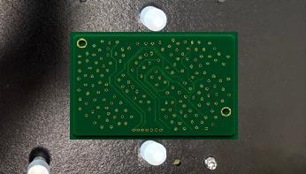
Guiding holes are critical for ensuring accurate positioning of the PCB. There must be at least two guiding holes in the PCB, and these should always be complete drilled holes. “Half holes” at the PCB edges must be avoided, as they do not provide the same positioning precision as fully drilled holes.
The diameter of guiding holes should be at least 3 mm. It is important that the PCB specification clearly states that these holes must be drilled and not milled, as drilled holes offer significantly better dimensional and positional tolerance.
To maximize fixture precision, guiding holes should be placed as far apart as possible. The greater the distance between them, the higher the positioning accuracy in the test fixture. Plated guiding holes should be avoided, since plating thickness may vary between production batches and affect dimensional consistency.
No high components should be placed around the guiding holes on the fixture bottom side of the PCB. Components in these areas risk being damaged when the board is inserted into the production test fixture.
For correct orientation, guiding holes should be placed asymmetrically. By adding a mechanical blocker in the fixture, the operator is forced to insert the PCB in the correct orientation, reducing handling errors and increasing repeatability.
PCB test points for reliable circuit board testing
The recommended minimum test point diameter is 1.0 mm, with an absolute minimum of 0.89 mm. The distance between test points should be at least 50 mil (1.27 mm).
If possible, place ALL the test-points on the same side of the PCB. This will be the bottom-side when the board is placed in the fixture. A fixture that has all the test-points on the bottom-side is much cheaper than a fixture that can connect to the DUT from both sides.
It is OK or even better to use plated holes as test-points. If needed, these can be connected from both sides of the PCB.
Via-holes shall NOT be used as test-points, it will cause insufficient contact and lot of problems.
Try to not place test-points close to THM-components, there is a risk that the selective soldering will cover the test-points with flux and generate connection-problems between the probe and the test-point.
There is normally no need to create test-points for signals/voltages at THM-component-pins. It is possible to put fixture-probes directly onto the THM-component-pins.
There is normally no need to put test-points on oscillators or crystals, and that can cause functional problems for the product. This can apply to other signals as well (be careful with adding test-points on important signals that are sensitive, this can cause an instable product).
It is normally a good idea to have test-points for all the supply-voltages, boot-signals and reset-signals. It is also good to have several test-points for GND. Signals/voltages in FFC-connectors must have test-points (it is not preferable to build test-fixtures that requires FFC-cables).
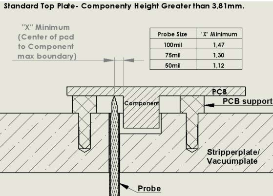
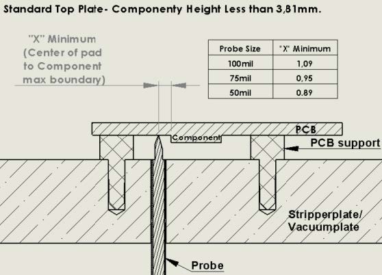
Test-fixture manufacturers require a specific distance between a test-probe and DUTcomponents beside the test-point. The required distance depends on the height of the component and thickness of the test-probe. These guidelines are based on fixture drilling requirements and not on any board related keep-out requirement (which may require even more distance). In the two pictures below, you find an example of the fixture manufacturer Columbia requirements in mm (the pictures are from Columbias document “Design for Testability Guidelines” Revision A).
Enough space between the centre of a guiding hole and the centre of a test-point is also required. This requirement is related to a need for space when using a specific insertion tool when assembling the fixture. As an example, Columbia requires a minimum of 7 mm.
PCB silk marking for efficient production testing
Silk marking on the PCB significantly improves production efficiency and reduces operator errors.
Each test point should be marked with its corresponding number in the silk layer. Pin 1 must be clearly indicated for all connectors and polarized components. It is also recommended to mark pin 2 and the last pin number on connectors to simplify troubleshooting and validation during production testing.
Important to know if the product shall be coated
If the product shall be coated it is important to try to keep test-points at areas where there is no need for coating. Then it will be possible to test coated units like reclaims from the field.
If the product shall have a housing
If the product shall have a housing it is a good idea to evaluate if there is a need for production test after the assembly of the housing. In that case the housing may need holes for test-probes and guiding pins, and this may have impact of the positioning of the test-points and guiding holes of the PCB.
Downloads
Design Guidline
AB0230-007, rev A. Design Guidline for production test.pdf
A trusted partner in electronic manufactures
With many years of experience in production testing, WireFlow deliver reliable PCB testing solutions and modular platforms that scale with your needs, improving quality, reducing costs, and ensuring full traceability.


